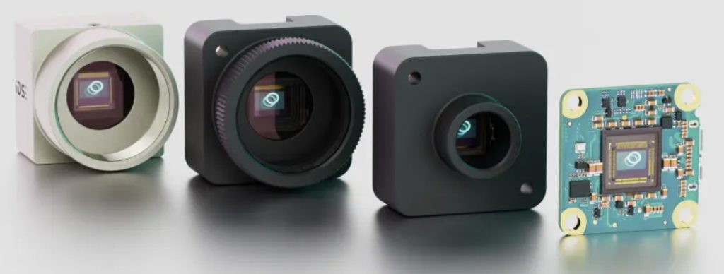
IDS Imaging will soon release new members in their uEye+ camera series, utilizing Sony’s 4th generation Pregius S sensors. Included are 16, 20, and 24 MP offerings of the compact uEye+ USB3 cameras.
The “S” in Pregius S stands for “stacked”, a sensor architecture that is back-illuminated as well as layered, creating a light-sensitive, low-noise, high-performance sensor. Even the first 3 generations of Sony Pregius sensors broke new ground, but Pregius S is special. Read our dedicated blog on the Sony Pregius four generation offerings, including details on Pregius S.
Sony Pregius S sensor
MP
Format
IMX 532
16
5328 x 3040
IMX 531
20
4512 x 4512
IMX 530
24
5328 x 4608
Sony Pregius S sensors joining IDS uEye+ family
IDS peak SDK : “Configuring instead of programming”
Enhancing the ease of development and deployment for the uEye+ cameras, IDS has released update 2.6 of “IDS peak”, the comprehensive software development kit (SDK), available at no cost. Of course the cameras are Vision Standard compatible ( U3V and GenICam), for those preferring third party SDKs, but IDS peak has much to offer IDS’ camera users.
While the SDK naturally includes conventional programming interfaces, IDS includes tools such as tools such as histograms, line and pixel views, color and greyscale conversions, useful automatic functions and bandwidth management. These skew deployment helpfully towards “configuring instead of programming”.
IDS peak is available for both Windows and Linux OS. In addition, IDS peak SDK works not just with IDS USB3 cameras, but also IDS GigE cameras. So multi-camera applications with mixed interfaces are possible. Or your developers can benefit from familiarity with a single SDK across multiple applications, bringing efficiencies to your team. Download IDS SDKs here.
Call us at 978-474-0044. Tell us about your applications goals and constraints, and we can guide you to any or all of cameras, lenses, lighting, software, and accessories.
Newer is better, right? Well yes if by better one wants the very highest performance. More below on that. But the predecessor generations are performant in their own right, and remain cost-effective and appropriate for many applications. We’re often get the question “What’s the difference?” – in this piece we summarize key differences among the 4 generations of SONY Pregius sensors.
In machine vision, sensors matter. Duh. As do lenses. And lighting. It’s all about creating contrast. And reducing noise. Each term linked above takes you to supporting pieces on those respective topics.
This piece is about the four generations of the SONY Pregius sensor. Why feature a particular sensor manufacturer’s products? Yes, there are other fine sensors on the market, and we write about those sometimes too. But SONY Pregius enjoys particularly wide adoption across a range of camera manufacturers. They’ve chosen to embed Pregius sensors in their cameras for a reason. Or a number of reasons really. Read on for details.
Machine Vision cameras continue to reap the benefits of the latest CMOS image sensor technology since Sony announced the discontinuation of CCD’s. We have been testing and comparing various sensors over the years and frequently recommend Sony Pregius sensors when dynamic range and sensitivity is needed.
If you follow sensor evolution, even passively, you have probably also seen a ton of new image sensor names within the “Generations”. But most users make a design-in sensor and camera choice, and then live happily with that choice for a few years. As we do when choosing a car, a TV, or a laptop. So unless you are constantly monitoring the sensor release pipeline, its hard to keep track of all of Sony’s part numbers. We will try to give you some insight into the progression of Sony’s Pregius image sensors used in industrial machine vision cameras.
How can I tell if it’s a Sony Pregius sensor?
Sony has prefixes of the image sensors which make it easy to identify the sensor family. All Sony Pregius sensors have a prefix of “IMX.” Example: IMX174 – which today is one of the best sensors for dynamic range..
What are the differences in the “Generations” of Sony Pregius Image sensors?
Sony Pregius Generation 1:
Primarily consisted of a 2.4MP resolution sensor with 5.86um pixels BUT had a well depth (saturation capacity) of 30Ke- and still unique in this regard within the generations. Sony also brought the new generations to the market with “slow” and “fast” versions of the sensors at two different price points. In this case, the IMX174 and IMX249 were incorporated into industrial machine vision cameras providing two levels of performance. Example being Dalsa Nano M1940 (52 fps) using IMX174 vs Dalsa Nano M1920 (39 fps) using IMX249, but the IMX249 is 40% less in price.
Sony Pregius Generation 2:
Sony’s main goal with Gen 2 was to expand the portfolio of Pregius sensors which consists of VGA to 12 MP image sensors. However, the pixel size decreased to 3.45um along with well depth to ~ 10Ke-, but noise also decreased! The smaller pixels allowed smaller format lenses to be used saving overall system cost. However this became more taxing on lens resolution being able to resolve the 3.45um pixels. In general it offered a great family of image sensors and in turn an abundance of machine vision industrial cameras at lower cost than CCD’s with better performance.
For Gen 3, Sony took the best of both the Gen 1 and Gen 2. The pixel size increased to 4.5um increasing the well depth to 25Ke-! This generation has fast data rates, excellent dynamic range and low noise. The family will ranges from from VGA to 7.1MP. Gen 3 sensors started appearing in our machine vision camera lineup in 2018 and continued to be designed in to cameras for the last few years.
Sony Pregius Generation 4:
The 4th generation is denoted Pregius S, and is designed in to a range of cameras from 5 through 25 Megapixels. Like the prior generations, Pregius S provide global shutter for active pixel CMOS sensors using Sony Semiconductor’s low-noise structure.
New with Pregius S is a back-illuminated structure – this enables smaller sensor size as well as faster frame rates. The benefits of faster frame rates are self-evident. But why is smaller sensor size so important? If two sensors, with the same pixel count, and equivalent sensitivity, are different in size, the smaller one may be able to use a smaller lens – reducing overall system cost.
Pregius S benefits:
With each Pregius S photodiode closer to the micro-lens, a wider incident angle is created. This admits more light. Which enhances sensitivity. At low incident angles, the Pregius S captures up to 4x as much light as Sony’s own highly-praised 2nd generation Pregius from just a few years ago!
With pixels only 2.74um square, one can achieve high resolution even is small cube-size cameras, continuing the evolution of more capacity and performance in less space.
Fun fact: The “S” in Pregius S is for stacked, the layered architecture of the sensor with the photodiode on top and circuits below, which as note has performance benefits. It’s such an innovation – despite already high-performing Gens 1, 2, and 3, that Sony graced Gen 4 as the Pregius S to really call out the benefits.
Summary
While Pregius S sensors are very compelling, the prior generation Pregius sensors remain and excellent choice for many applications. It comes down to performance requirements and cost, to achieve the optimal solution for any given application.
Many Pregius sensors, including Pregius S, can be found in industrial cameras offered by 1stVision. Use our camera selector to find Pregious sensors, any staring with “IMX”. For Pregius S in particular, supplement that prefix with a “5”, i.e. “IMX5”, to find Pregious S sensor like IMX540, IMX541, …, IMX548.
Sometimes just the Z-values are enough, no image needed at all. Some applications require pseudo-images generated from a point cloud – whether in monochrome or with color tones mapped to Z values. Yet other applications require – or benefit from – 3D digital point cloud data as well as color rendering. IDS Ensenso’s C Series provides stereo 3D imaging with precise metrics as well as true color rendering.
If you want an overview of 3D machine vision techniques, download our Tech Brief. It surveys laser triangulation, structured light, Time of Flight (ToF), and stereo vision. If you know you want stereo vision, you might like an overview of all IDS Ensenso 3D offerings.
But if you know you want stereo 3D accuracy to 0.1mm, with color rendering, let’s dive in to the IDS Ensenso C Series. If you prefer to speak with us instead of reading further, just call us at 978-474-0044, or request that we follow up via our contact form.
Key differentiator is “projected texture”
In the short video below, we see 3 scene pairs. For each pair, the leftmost images are the unenhanced 3D image. The rightmost images take advantage of the projected texture created by the LED projector and the RGB sensor, augmenting the 3D point cloud with color information. It can be a differentiator for certain applications.
Application areas
Let’s start with candidate application areas, from customer perspective, before pointing out specific features. In particular let’s look at application areas including:
Detect and recognize
Bin picking
De-palletizing
Test and measure
Detect and recognize
The ability to accurately detect moving objects to select, sort, verify, steer, or count can enhance (or create new) applications. Ensenso C’s high-luminance projector enables high pattern contrast for single-shot images. Video courtesy of IDS.
Bin picking
Regardless of a robot’s gripping sensitivity, speed, and range of motion, 3D imaging accuracy is central to success. Ensenso C’s integrated RGB sensor can make all the difference for color-dependent applications. Video courtesy of IDS.
De-palletize
De-palletizing might seem like a straightforward operation, but must detect object size, rotation and position even with different and densely stacked goods. Ensenso C supports all those requirements – even from a distance. Video courtesy of IDS.
Test and measure
Automated inspection and measurement of large-volume objects are key for many quality control applications. Precision to the millimeter range can be achieved with Ensenso C at working distances even to 5m. Video courtesy of IDS.
IDS Ensenso C Series
With two models to choose from, Ensenso C supports a range of working distances and focal distances – see specifications.
Both models utilize GigE Vision interface; both embed a 200W LED projector; both use C-mount lenses; both provide IP 65/67 protection. And both models are easy to configure with the Ensenso SDK: Windows or Linux; sample programs including source code; live composition of 3D point clouds from multiple viewing angles; robot eye-hand calibration; and more.
Have you wondered if 3D laser profiling would work for your application? Unless you have experience in 3D imaging, for which laser profiling is one of several popular methods, you may be uncertain of the fit for your application. Yes, one can read a comprehensive Tech Briefs on 3D methods, or product specifications, but wouldn’t it be helpful to see some images of your parts taken with an actual 3D Laser Profiler?
While prototyping at your facility is of course one option, if your target objects can be shipped, Teledyne DALSA has a Z-Trak Application Lab, whose services we may be able to arrange at no cost to you. Just describe your application requirements to us, and if 3D laser profiling sounds promising, the service works as follows:
Send in representative samples (e.g. good part, bad part)
We’ll configure Z-Trak Application Lab relative to sample size, shape, and applications goals, and run the samples to obtain images and data
We’ll send you data, images, and reports
Together we’ll interpret the results and you can decide if laser profiling is something you want to pursue
Really, just send samples in? Anything goes? Well not anything. It can’t be 50 meters long. Maybe a 15 centimeter subset would be good enough for proof of concept? And if the sample is a foodstuff, it can’t suffer overnight spoilage before it arrives.
A phone conversation that discusses the objects to be inspected, their dimensions, and the applications goal(s) is all we need to qualify accepting your samples for a test. Image courtesy of Teledyne DALSA.
Case study
In this segment, we feature outtakes from a recent use of the Z-Trak Application Lab, for a customer who needs to do weld seam inspections. The objective is to image a metal part with two weld seams using a Z-Trak 3D Laser Profiler and produce 3D images for evaluation of application feasibility. The images and texts shown here are taken from an actual report prepared for a prospective customer, to give you an understanding of the service.
Equipment:
Z-Trak LP1-1040-B2
Movable X,Y stage X-Resolution: ~25 um Y-Resolution: 40 um WD: ~50 mm
Image courtesy Teledyne DALSA
Conditions: The metal part was laid flat on the X,Y stage under the Z-Trak. The stage was moved to scan the part.
To the right, see the image generated from a perpendicular scan of the metal part. Image courtesy Teledyne DALSA.
The composite image below requires some explanation. The graphs on the middle column, from top to bottom, show Left-Weld-Length, Right-Weld-Length, and Weld-Midpoint-Width (between the left and right welds), respectively. The green markup arrows help you correlate the measurements to the image on the left. The rightmost column includes summary measurements such as Min, Max, and Mean values.
Now have a look at a similar screenshot, for Sample #2, which includes a “bad weld”:
With reference to the image above, the customer report included the following passage:
The top-right image is the left weld seam profile. In the Reporter window the measurement of this seam is 1694.79 mm long. However, a defect can be noted at the bottom of the left weld. In addition to the defect it can be seen from the profile that the weld is not straight in the Z-direction. The weld is closer to the surface at the top and further from the surface at the bottom
Translation: The automated inspection reveals the defective weld! Naturally one would have to dig in further regarding definitions of “good weld”, “bad weld”, tolerances, where to set thresholds to balance yields and quality standards vs. too many false positives, etc.
Conclusion
The report provided to the customer concluded that “This application is feasible using a Z-Trak 3D Laser Profiler.” While it’s likely that outcome will be achieved if we qualify your samples and application to use the Z-Trak Application Lab service, it’s not a foregone conclusion. We at 1stVision and our partner Teledyne DALSA are in the business of helping customers succeed, so we’re not going to raise false hopes of application success.
Recap
To summarize, the segments above are representative outtakes from an actual report prepared by the Z-Trak Application Lab. The full report contains more images, data, and analysis. Our goal here is to give you a taste for the complimentary service, to help you consider whether it might be helpful for your own application planning process.
If you’d like to send in your parts, please use this “Contact Us” link or the one below. In the ‘Tell us about your project’ field, just write something like “I’d like to have parts sent to the Z-trak lab.” If you want to write additional details, that’s cool – but not required. We’ll call to discuss details at your convenience.