IDS Software Suite 4.96.1
 |
NOTICE! Make sure to avoid mechanical or electrical damage of the printed circuit board or its connections. Do not touch the printed circuit board while it is powered. Always hold the board by the edges to avoid the risk of electrostatic discharge damage. |
 |
The applicable tolerances for the overall dimensions of PCBs are higher than the tolerances for housing dimensions. |
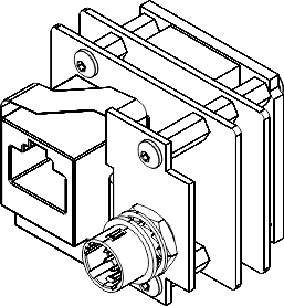
 with CMOS - 3D view") Fig. 680:GigE uEye SE OEM version 2 (PCB stack) with CMOS - 3D view |
 |
CMOS/CCD cameras
 Fig. 681: GigE uEye SE OEM version 2 - Front view |
 Fig. 682: GigE uEye SE OEM version 2 - Rear view |
CCD cameras
") Fig. 683: GigE uEye SE OEM version 2 - Top view (CCD) |
") Fig. 684: GigE uEye SE OEM version - Side view (CCD) |
CMOS version
") Fig. 685: GigE uEye SE OEM version 2 - Top view (CMOS) |
") Fig. 686: GigE uEye SE OEM version 2 - Side view (CMOS) |